Tools & Platforms
Microsoft, US national lab tap AI to speed up nuclear power permitting process
“It’s created for human refinement, so a human can go through each of the sections and, specifically as needed, edit any of the sections, whether manually, or maybe with the help of AI – it’s really up to the human,” Nelli Babayan, AI director for federal civilian business at Microsoft, told Reuters in an interview.
The move comes after President Donald Trump in May signed executive orders to fast-track the licensing process for new nuclear power plants, aiming to shorten what is often a multiyear process into as little as 18 months as AI data centers create soaring demand for energy.
The technology could also help with squeezing more energy out of existing nuclear plants, said Scott Ferrara, deputy division director for nuclear safety and regulatory research at INL. Existing nuclear facilities must submit an evaluation of how they might increase power output and apply for an amendment to their operating license.
“A plethora of data already exists from about 82 upgrades that have already taken place, and they can just pull right from that (data) and help generate their license amendment request,” Ferrara told Reuters in an interview.


Tools & Platforms
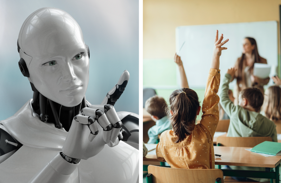
China is making AI education mandatory for kids – and it’s already rolling out in schools
Artificial intelligence is rapidly becoming part of our everyday routines. Whether it’s checking in with ChatGPT, using Face ID to unlock phones, or a subtle tweak to photos before sharing them online, AI is there behind the scenes.
With no sign of this slowing down, a school in China is moving quickly to prepare its pupils by making AI education compulsory.
In Hangzhou, Zhejiang province, authorities have introduced compulsory AI education for all primary and secondary students, aiming to get ahead of the curve and equip children with essential knowledge of the technology.
From this term, schools are reportedly expected to add at least 10 hours of AI lessons each academic year. They will have the flexibility to decide how to deliver the content – whether through an intensive week-long course or by integrating AI topics across different science and technology classes, according to South China Morning Post.
The new curriculum sets out a step-by-step approach to AI education, gradually building students’ skills from the earliest years of school.
In the first two years of primary, children will be introduced to AI through familiar tech, like smart speakers or facial recognition, and taught the basics of responsible use, with an emphasis on privacy.
iStock
By Years 3 and 4, they’ll begin using AI tools to collect and combine text, images and audio for simple projects, applying the technology to everyday tasks. Years 5 and 6 go deeper, with students learning about core concepts like decision trees, neural networks and basic algorithms.
In middle school, the focus shifts to real-world applications. Students will work through the full AI workflow, from data preparation to model training, and learn to evaluate technologies like generative AI.
By high school, the curriculum becomes project-based. Pupils will design their own AI systems and intelligent agents, applying what they’ve learnt to practical challenges.
Though still early in its rollout, the programme reflects China‘s wider goal to lead in AI – starting by making it second nature for the next generation.
You should also read…
Sign up to our free Indy100 weekly newsletter
How to join the indy100’s free WhatsApp channel
Have your say in our news democracy. Click the upvote icon at the top of the page to help raise this article through the indy100 rankings.

In the rapidly evolving world of semiconductors, Samsung Electronics Co. is navigating a complex web of challenges and opportunities as it heads into the latter half of 2025. The South Korean tech giant, a key player in memory chips and foundry services, has been grappling with supply chain disruptions and intense competition from rivals like TSMC and Intel. According to a recent report from Samsung Securities, the company faces difficulties in upward earnings revisions for general-purpose semiconductors due to ongoing production controls aimed at accelerating cycle recovery. This caution stems from uncertain capital expenditure (Capex) and utilization rate forecasts, which investors are watching closely for signs of a bottom-out.
Samsung’s strategic investments, however, signal a bold push forward. The company recently held a tool-in ceremony for its new semiconductor R&D complex, NRD-K, set to begin operations this year, with plans to pour about 20 trillion won ($14.8 billion) into advanced R&D by 2030, as detailed in the Samsung Global Newsroom. This move is part of a broader effort to bolster AI-driven semiconductors, where Samsung sees higher earnings visibility amid the global AI boom.
Investors Eye AI as Samsung’s Lifeline Amid Market Pressures
First-quarter 2025 results underscored both strengths and vulnerabilities, with Samsung reporting revenue of 79.14 trillion won and operating profit of 6.7 trillion won, per the company’s own announcements in the Samsung Global Newsroom. Yet, shareholders have pressed for growth strategies, leading CEO Kyung Kye-hyun to hint at pursuing major mergers and acquisitions this year to counter underperformance in tech stocks, as covered by Reuters. The failure to fully capitalize on AI has been a sore point, with Samsung’s foundry business posting losses of $3.6 billion in the first half of the year, though a $16.5 billion deal with Tesla for AI chips starting in 2027 offers a glimmer of hope, according to posts circulating on X from industry analysts.
Beyond semiconductors, Samsung is innovating in consumer devices to diversify revenue. The foldable smartphone segment is heating up, with the company planning to strengthen its lineup, including the rumored Galaxy G-Fold tri-fold phone slated for a late-2025 launch, as revealed in leaks reported by Geeky Gadgets. This comes amid growing competition from Huawei and Google, with market overviews from Coherent Market Insights forecasting robust industry growth through 2032.
Strategic Shifts in Foundry and Packaging Technologies
Samsung’s ambitions extend to advanced packaging, where it’s exploring Intel’s hybrid bonding technology to enhance chip density and efficiency, as noted in recent X posts from tech enthusiasts like Techo Vedas. This could position Samsung better against TSMC, whose 2nm process is eyeing mass production in Q4 2025 with a monthly capacity of 100,000 wafers by 2026, according to semiconductor news aggregated on X by inni world. Meanwhile, Samsung’s own 2nm advancements are crucial for reclaiming market share, especially as global wafer foundry revenue surged 14.6% to $41.7 billion in Q2, with TSMC dominating over 70% of the market.
The company’s mobile division is also adapting, with expectations for a delayed flagship processor launch and expanded Galaxy AI features across premium devices, as outlined in X updates from insider Anthony. Price increases for components and a focus on thinner, redesigned foldables aim to counter Apple’s rumored 2026 entry into the foldable arena, per Business Insider.
Geopolitical Tensions and Supply Chain Resilience
Geopolitical factors add another layer of complexity. China’s record chip exports of $89.85 billion in the first seven months of 2024, despite U.S. sanctions, highlight shifting dynamics that could pressure Samsung, as discussed in X posts by Barrett. Samsung’s response includes bolstering domestic capabilities, such as the joint task force for a Galaxy-only chip by 2025, echoing earlier strategies reported in X threads from Anthony dating back to 2022.
Looking ahead, Samsung’s semiconductor outlook hinges on AI recovery evidence, with traditional equipment investments poised to rebound once cycle improvements materialize, per the Sourceability analysis. The resolution of excess inventory is paving the way for growth, but challenges like Intel’s Arrow Lake setbacks and Huawei’s R&D surges, as per X semiconductor news from inni world, underscore the need for agility.
Innovation Beyond Chips: Foldables and Emerging Tech
In foldables, Samsung’s Galaxy Z Fold 7 and Flip models are stacking up well against competitors like Motorola and Google, with expert reviews from ZDNet praising next-gen features. The tri-fold Galaxy G-Fold, detailed in Gadget Hacks, promises to redefine multitasking with its expansive
Tools & Platforms
[News] TSMC Partners with Technical University of Munich to Establish AI Chip R&D Center in Bavaria

According to Liberty Times, citing German media outlet BR24, the Bavarian state government has announced a collaboration with TSMC to establish an AI chip research and development center at the Technical University of Munich (TUM).
The center, officially named the Munich Advanced-Technology Center for High-Tech AI Chips (MACHT-AI), will be led by Professor Hussam Amrouch of TUM. As the report indicates, the move deepens cooperation with TSMC and seeks to strengthen Europe’s chip design capabilities.
The report notes that funding for the AI chip R&D center will come jointly from Bavaria’s Ministry of Science and Ministry of Economic Affairs, with a total budget of about EUR 4.5 million.
For this AI chip center, the report highlights that TSMC will provide technical support, focusing on the development of high-performance, customizable AI chips, while also training students and researchers in manufacturing processes such as FinFET.
As the report mentions, in May TSMC announced at the Europe Technology Symposium that it would establish a chip design center in Munich to help European customers develop high-performance chips for automotive, artificial intelligence, and industrial IoT applications, with operations slated to begin in the third quarter of this year.
eeNews Europe indicates that TSMC’s decision to set up a chip design center in Europe may have been motivated by the region’s shortage of advanced design expertise and the need to provide close support for customers in maximizing the value of the wafer fab it is building in Dresden.
In August 2024, ESMC—TSMC’s joint venture with Bosch, Infineon, and NXP—broke ground in Dresden on what will be the EU’s first FinFET-capable pure-play foundry. When fully operational, ESMC is expected to produce 40,000 300mm (12-inch) wafers per month on TSMC’s 28/22nm planar CMOS and 16/12nm FinFET process technologies, as its press release indicates.
Read more
(Photo credit: TSMC)
Please note that this article cites information from Liberty Times, BR24, the Bavarian state government, eeNews Europe, and TSMC.

-

 Business4 days ago
The Guardian view on Trump and the Fed: independence is no substitute for accountability | Editorial
-
Tools & Platforms3 weeks ago
Building Trust in Military AI Starts with Opening the Black Box – War on the Rocks
-

 Ethics & Policy1 month ago
SDAIA Supports Saudi Arabia’s Leadership in Shaping Global AI Ethics, Policy, and Research – وكالة الأنباء السعودية
-

 Events & Conferences3 months ago
Journey to 1000 models: Scaling Instagram’s recommendation system
-

 Jobs & Careers2 months ago
Mumbai-based Perplexity Alternative Has 60k+ Users Without Funding
-
 Funding & Business2 months ago
Kayak and Expedia race to build AI travel agents that turn social posts into itineraries
-
 Education2 months ago
VEX Robotics launches AI-powered classroom robotics system
-

 Podcasts & Talks2 months ago
Happy 4th of July! 🎆 Made with Veo 3 in Gemini
-

 Education2 months ago
AERDF highlights the latest PreK-12 discoveries and inventions
-

 Podcasts & Talks2 months ago
OpenAI 🤝 @teamganassi