AI Insights
Artificial intelligence drives the demand for the electric grid – Fox News


Saturday, September 06, 2025
University of Rhode Island men’s basketball coach Archie Miller is at the forefront of utilizing AI-powered technology to support the basketball program, and a URI alum is helping to make it happen.
AI technology is everywhere, and marketers love the term, with even routine, static computer programs being referred to as “AI.” The application URI is using claims to be robust, deeply technical, data-rich, with independent program learning, and is a highly advanced artificial intelligence application.
GET THE LATEST BREAKING NEWS HERE — SIGN UP FOR GOLOCAL FREE DAILY EBLAST
A URI Alum is behind this
Roby Luna graduated from URI in 2000 with a BS in MIS (Management Information Systems). He is the President and one of the founders of Aretec, Inc., which is a technology company that provides data science, cloud services, and AI-powered solutions to government agencies and commercial clients. It specializes in using data to improve decision-making.
That is what Luna does for a living. Here is what he does for fun. Luna is also a co-founder of Slam Sports AI. He and others have applied their expertise in mining, analyzing, and presenting data to support decision-making to the field of college basketball.
Miller’s comments on the value of the AI platform
When asked about their AI initiative and Luna, Coach Miller said, “The technology created by Slam Sports offers a cutting-edge tool for player-performance evaluation. On and off the court, the game is moving faster than ever. When you find a tool that can speed up various evaluation needs, it helps us become more efficient in all of our work.”
Miller continued, “As an alum, Roby Luna has a clear affinity for URI. When he presented the potential uses of Slam Sport, being a part of this pilot program made sense. His understanding of data analytics and how it could benefit the basketball program made this a very useful tool.”
How does it work?
Slam Sports harvests videos of college basketball players and uses a proprietary AI software platform that “reads” and analyzes video to produce individual scouting reports on players. Coaches no longer have to spend hours and hours watching films to develop an assessment of a prospect. Instead, they receive a detailed and customized data-driven report on every prospect they are interested in.
This time-saving service is incredibly valuable in the era of the Transfer Portal, where a team may be looking at 100 players and has a short time to make decisions.
The data analysis and report on each player includes several items, including.
Foot speed
Athleticism
Acceleration
Passing accuracy
Decision making
Shooting from different distances
Movement without the ball
Off-ball defense
Transition from offense to defense
Transition from defense to offense
Reaction to missed shots
And more
The report on a player also includes “Sentiment Analysis.” Under this heading, factors such as body language, the player’s reaction when they are beaten on defense, their reaction when taken out of a game, a player’s mannerisms after a coach talks with them, how a player behaves on the bench, and other physical responses to activities on the court.
Wait, there is more
The player analysis and reports are not simply based on the athlete’s general performance. The analysis is based on a customized platform of Miller’s specific preferences for each aspect of playing basketball.
After lengthy discussions with Miller, Slam Sports creates a digital agent – an avatar, if you will, which represents Miller’s thesis for every component of playing basketball. A player’s performance is analyzed against Miller’s digital agent.
The software program that completes this task is high-level AI as it self-learns, refining its program and evolving as it analyzes players against the avatar.
Example of the AI platform in use
During this transfer period, URI was looking for a big man. They were aware of a center that played overseas. Traveling overseas to see a player firsthand is not something URI is going to do. Traditionally, coaches would review game films. However, a player’s performance is highly dependent on the talent level they are playing against, which can sometimes be difficult to determine when only watching film.
Slam Sports ran the player’s game film through their program and within minutes produced an analysis. The report revealed that the player’s foot speed and athleticism were insufficient to be competitive in the A-10, and his decision-making was suspect. URI moved off this player, saving time and avoiding the waste of NIL money and a roster spot.
Recruiting from the portal
This year, 2,700 college basketball players entered the transfer portal. That is an enormous number of players to look at and analyze. The first step for a basketball program is to identify the players it has the potential to recruit. The coaching staff then focuses on a selected group of players. If last year, URI focused on 100 to 200 players with the AI tool, they can look at twice as many and do it quickly.
Slam Sports also provides the service of identifying players whom URI may have overlooked. In harvesting their player data, Slam Sports may find a qualified player that URI did not have on its list to explore.

URI player evaluations
The AI analytics tool is also being used to evaluate current URI players for the purpose of player development. Basketball practices are videotaped and, along with game footage, are run through the AI program. Coaches and players receive detailed reports, which are used to identify specific areas for improvement that will be tracked throughout the year.
Scouting opponents
Slam Sports has been collecting videos of players on the teams URI will be competing against this year. These videos, along with current game videos, will be used to analyze opponents, producing a data-rich but consumable scouting report prior to every game.
More about Luna
Luna provides Slam Sports AI services to URI at no cost. It’s his way of giving back to the University he loves and feels indebted to. Luna’s parents immigrated to the United States from the Dominican Republic when he was a young boy. He grew up in Providence, attending Central High School.
He was a gifted athlete with dreams of playing in Major League Baseball. However, he lost his singular focus on this goal and succumbed to distractions. So, it was off to the U.S. Army after high school.
After his time in the armed services, URI’s Talent Development Program, which is designed to give students from underperforming high schools or with disadvantaged backgrounds the opportunity to attend URI, became aware of Luna and accepted him into the program.
In talking about the Talent Development Program, Luna said, “I was ill-prepared for the rigors of college. But my advisor at the time, Sharon Forleo, was instrumental in helping me to stay the course. I am forever grateful to her for helping me push forward and try to achieve my dream of making a dent in the universe.”
Luna further said, “I will forever bleed Rhody blue.” In addition to these latest efforts with the basketball team, Luna serves on the URI Board of Trustees and Chairs the Committee on Institutional Risk and Compliance.
What’s next
Luna believes his AI program and analysis system are capable of providing real-time in-game analysis. The first five minutes of a game are generally a time when teams are feeling each other out, and coaches are evaluating how their game strategy is working. Although Slam Sports does not currently have the functionality, Luna envisions that in the near future, after the first five minutes of a game, the coaching staff will be given a detailed analysis of the game generated by its AI platform.
Real or magic
So, is this all real, or is it magic? Was Luna the lucky one who was walking across the Quad and found the pouch of magic dust some wizard left behind? Or has this all happened due to the intersection of hard work, perseverance, and the award-winning Talent Development Program at URI?
You will need to decide.

James Malachowski is the former Chairman/Managing Partner at RDW Group. He previously served as the chair of the Public Utilities Commission. He is a graduate of URI and PC.
Related Articles
Enjoy this post? Share it with others.
AI Insights
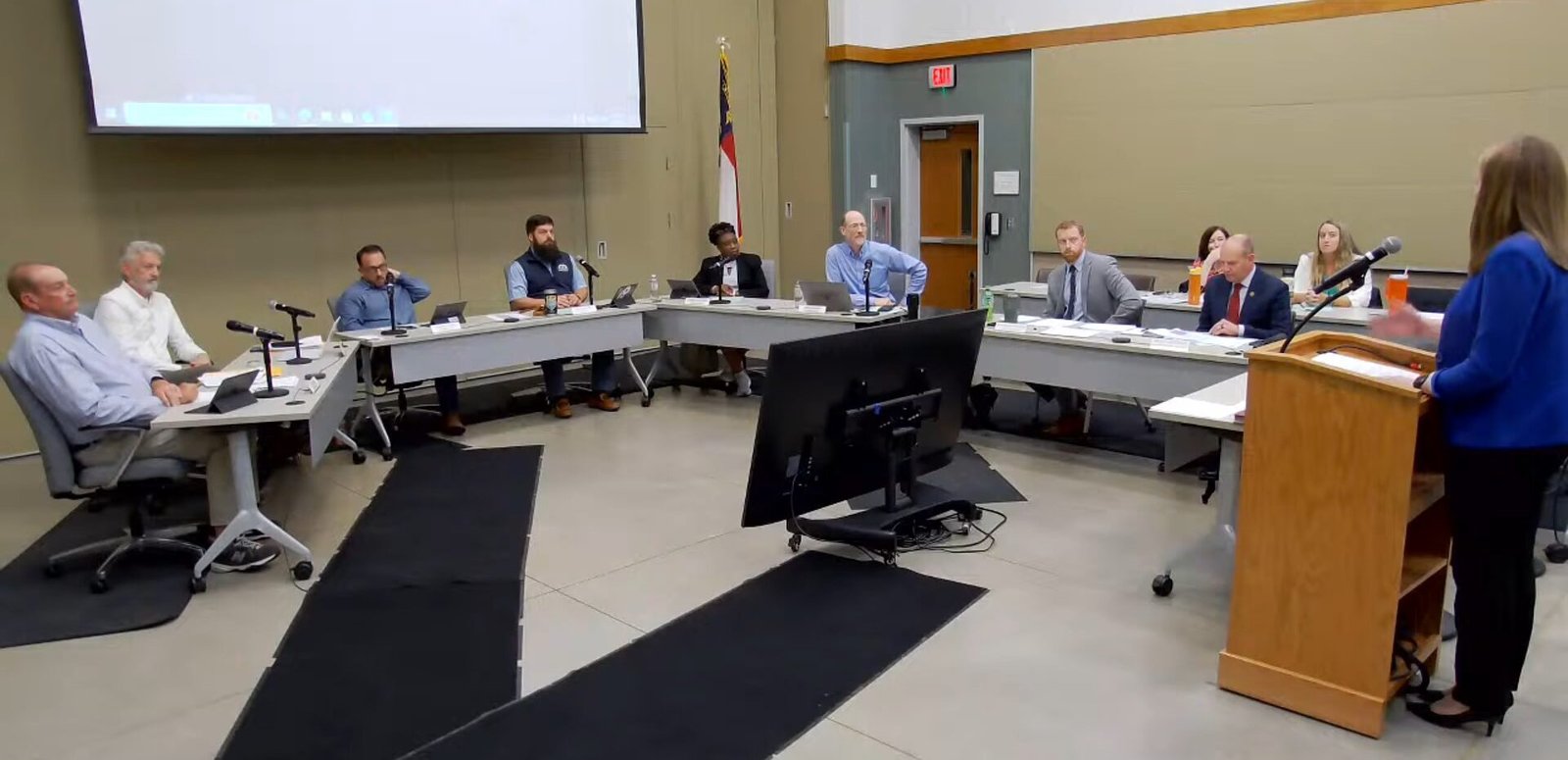
Artificial Intelligence Consultant Ashley Gross Shares Details on Pittsboro Commissioner Candidacy

Among the eight candidates looking to connect with voters in Pittsboro this fall is Ashley Gross, an artificial intelligence advocate, consultant and course creator.
Gross filed to run for the town government’s Board of Commissioners in July, joining a crowded race to replace the outgoing Pamela Baldwin and James Vose. A resident of the Vineyards neighborhood of Chatham Park, she works as a keynote speaker and consultant for businesses looking to learn more about AI practices in the emerging technology space, leading her own consulting company and working as the CEO of the organization AI Workforce Alliance.
In an email with Chapelboro, Gross described herself as “a mom who loves this little corner of the world we call home” and committed to the area. When describing her motivation to run — in which she incorrectly stated she was running for a county commissioner seat — she said helping the greater Pittsboro community feel connected and supported with a variety of resources is key amid the town’s ongoing growth.
“I see the push and pull between people who have called Chatham home for generations and those who are just discovering it,” Gross said. “I believe that our differences are not barriers. They are opportunities to learn from each other. My strength is sitting down with people, even when we disagree, and finding the common ground we share. I am a researcher and an experimenter by nature, and I have seen that the most successful communities are built when people come together around shared interests and goals. That is the kind of leadership I want to bring, one that unites us instead of dividing us.”
Gross cited uplifting small businesses to help maintain the local economy as a key priority, as well as public safety and investments into local infrastructure.
“Safe roads, modern emergency response systems, and preparation for the weather risks we face mean families can feel secure no matter what comes our way,” she said. “And as we grow, I will focus on smart development that keeps our small town character intact while building the infrastructure we need for the future.”
Other priorities the Pittsboro resident listed as having strong local schools, improving partnerships with local colleges and expanding reliable internet to each home and business — all issues that fall more under the purview of the Chatham County government more than the town government.
When describing what she is looking forward to during her campaign for Pittsboro’s Board of Commissioners, Gross wrote that she wants to hear directly from residents about their “concerns, hopes and ideas” while listening and using “data and common sense” to inform her policy decisions.
“Every choice I make,” Gross wrote, “will be guided by a simple question: will this keep our families safe, connected, and thriving? At the end of the day, I am just a mom who believes Chatham is at its best when we work as one community, where families stay close, opportunities grow here, and every neighbor feels they belong.”
Gross will be on the ballot along with Freda Alston, Alex M. Brinker, Corey Forrest, Candace Hunziker, Tobais Palmer, Nikkolas Shramek and Tiana Thurber. The top two commissioner candidates to receive votes will serve four-year terms on the five-seat town board alongside Pittsboro Mayor Kyle Shipp — who is running unopposed for re-election.
Election Day for the 2025 fall cycle will be Tuesday, Nov. 4, with early voting in Chatham County’s municipal elections beginning on Thursday, Oct. 10.
Featured image via Ashley Gross.
Chapelboro.com does not charge subscription fees, and you can directly support our efforts in local journalism here. Want more of what you see on Chapelboro? Let us bring free local news and community information to you by signing up for our newsletter.
Related Stories


Google DeepMind introduced a new artificial intelligence model that captures the vivid details of the Earth’s surface, which helps scientists and governments make better decisions about the land and sea.
-

 Business1 week ago
The Guardian view on Trump and the Fed: independence is no substitute for accountability | Editorial
-
Tools & Platforms4 weeks ago
Building Trust in Military AI Starts with Opening the Black Box – War on the Rocks
-

 Ethics & Policy1 month ago
SDAIA Supports Saudi Arabia’s Leadership in Shaping Global AI Ethics, Policy, and Research – وكالة الأنباء السعودية
-

 Events & Conferences4 months ago
Journey to 1000 models: Scaling Instagram’s recommendation system
-

 Jobs & Careers2 months ago
Mumbai-based Perplexity Alternative Has 60k+ Users Without Funding
-
 Education2 months ago
VEX Robotics launches AI-powered classroom robotics system
-

 Podcasts & Talks2 months ago
Happy 4th of July! 🎆 Made with Veo 3 in Gemini
-

 Funding & Business2 months ago
Kayak and Expedia race to build AI travel agents that turn social posts into itineraries
-

 Education2 months ago
Macron says UK and France have duty to tackle illegal migration ‘with humanity, solidarity and firmness’ – UK politics live | Politics
-

 Podcasts & Talks2 months ago
OpenAI 🤝 @teamganassi